| CPC G09G 3/3233 (2013.01) [H01L 27/1222 (2013.01); H01L 27/124 (2013.01); H10K 59/1213 (2023.02); G09G 2300/0819 (2013.01); G09G 2300/0861 (2013.01); G09G 2310/0251 (2013.01); G09G 2310/0262 (2013.01); H10K 59/1216 (2023.02); H10K 59/131 (2023.02)] | 1 Claim |
|
1. An organic light-emitting display apparatus, comprising:
a first scanning line;
a second scanning line;
a first voltage line;
a second voltage line; and
a pixel;
wherein:
the pixel comprises:
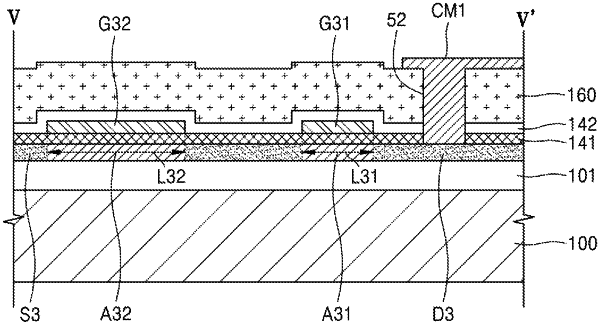
an organic light-emitting diode;
a semiconductor layer;
a first thin film transistor electrically connected to the organic light-emitting diode and the first voltage line;
a second thin film transistor electrically connected to the first thin film transistor and the first scanning line;
a third thin film transistor electrically connected to the second thin film transistor and the second voltage line, and electrically connected to the second scanning line; and
a fourth thin film transistor electrically connected to the third thin film transistor and the second voltage line;
the first thin film transistor, the second thin film transistor, the third thin film transistor, and the fourth thin film transistor are connected by the semiconductor layer;
the semiconductor layer is overlapped by the second scanning line in at least three portions; and
the second thin film transistor has two gate electrodes, which are a portion of the first scanning line and a portion protruding from the first scanning line, and overlap the semiconductor layer,
wherein:
a contact hole is defined in at least one insulating layer between the semiconductor layer and the second voltage line;
the contact hole is between the third thin film transistor and the fourth thin transistor in a plan view; and
the third thin film transistor and the fourth thin film transistor are connected to the second voltage line through the contact hole.
|