| CPC G09G 3/3233 (2013.01) [G09G 2300/043 (2013.01); G09G 2300/0819 (2013.01); G09G 2300/0842 (2013.01); G09G 2300/0861 (2013.01); G09G 2310/08 (2013.01); G09G 2320/0214 (2013.01); G09G 2320/0247 (2013.01); G09G 2330/021 (2013.01)] | 12 Claims |
|
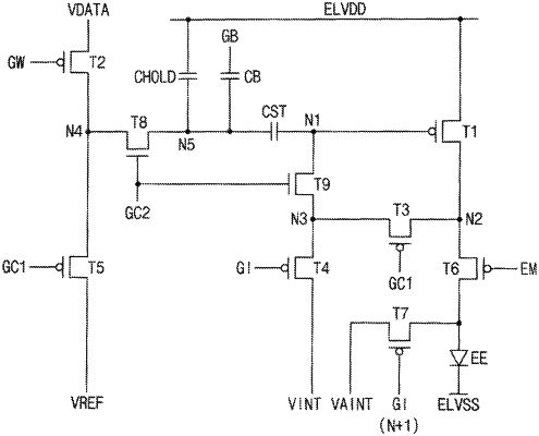
1. A display apparatus comprising:
a display panel comprising a pixel;
a gate driver which provides a gate signal to the pixel;
a data driver which provides a data voltage to the pixel; and
an emission driver which provides an emission signal to the pixel,
wherein the pixel comprises:
a light emitting element;
a driving switching element which applies a driving current to the light emitting element;
a storage capacitor connected to a control electrode of the driving switching element; and
a bias capacitor including a first electrode connected to the storage capacitor and a second electrode which receives a bias gate signal, and
wherein a waveform of the bias gate signal varies based on an off ratio representing a ratio of an off period of the emission signal in a frame period.
|