| CPC G09G 3/3225 (2013.01) [G11C 19/28 (2013.01); H10K 59/1213 (2023.02); H10K 59/124 (2023.02); H10K 59/131 (2023.02); H10K 71/00 (2023.02); G09G 2300/0426 (2013.01); G09G 2310/0286 (2013.01); H10K 59/1201 (2023.02)] | 20 Claims |
|
1. A display substrate, comprising:
a base substrate, comprising a display region and a peripheral region on at least one side of the display region; and
a shift register unit and a first clock signal line in the peripheral region of the base substrate, wherein the first clock signal line extends along a first direction on the base substrate, and is connected to a first clock signal terminal to be configured to provide a first clock signal to the shift register unit;
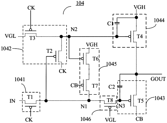
the shift register unit comprises an input circuit, an output circuit, a first control circuit, and an output control circuit;
the input circuit is configured to input an input signal to a first node in response to the first clock signal;
the output circuit is configured to output an output signal to an output terminal;
the first control circuit is configured to control a level of a second node in response to a level of the first node and the first clock signal;
the output control circuit is configured to control a level of the output terminal under control of the level of the second node;
the output control circuit comprises an output control transistor and a first capacitor, and the output circuit comprises an output transistor and a second capacitor;
an active layer of the output control transistor and an active layer of the output transistor are integrally provided and extend along the first direction;
the active layer of the output control transistor and the active layer of the output transistor provided integrally comprise a first output semiconductor layer and a second output semiconductor layer arranged side by side along a second direction different from the first direction, and an orthographic projection of the second output semiconductor layer on the base substrate is between an orthographic projection of the first output semiconductor layer on the base substrate and the display region;
an end, away from the display region, of the orthographic projection of the first output semiconductor layer on the base substrate comprises a first sub-notch; and
an end, close to the display region, of the orthographic projection of the second output semiconductor layer on the base substrate comprises a second sub-notch.
|