| CPC G09G 3/32 (2013.01) [G09G 2300/0426 (2013.01); G09G 2300/0819 (2013.01); G09G 2300/0842 (2013.01); G09G 2310/0278 (2013.01); G09G 2310/062 (2013.01); G09G 2310/08 (2013.01); G09G 2320/045 (2013.01)] | 13 Claims |
|
1. A display panel, comprising:
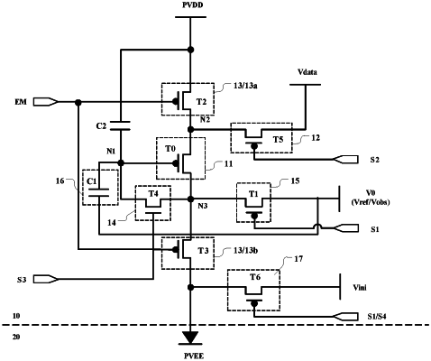
a pixel circuit and a light-emitting element, wherein:
the pixel circuit includes a driving module, a data-writing module, and a compensation module, and a reset module;
the driving module includes a driving transistor;
the data-writing module is connected to a source of the driving transistor and configured to selectively provide a data signal for the driving transistor;
the compensation module is connected between a gate and a drain of the driving transistor;
the reset module is connected between the drain of the driving transistor and a reset signal terminal and configured to provide a reset signal for the gate of the driving transistor;
the reset module is used as a bias module, an operating process of the pixel circuit includes a reset stage and a bias stage;
in the reset stage, the compensation module and the reset module are turned on, and the reset signal terminal provides the reset signal to the gate of the driving transistor;
in the bias stage, the compensation module is turned off, the reset module is turned on, and the reset signal terminal provided a bias signal to the drain of the driving transistor;
the pixel circuit further includes a latch module and a reset signal line, the reset signal line being configured to provide the reset signal or the bias signal for the reset signal terminal, and the latch module being connected between the gate of the driving transistor and the reset signal line;
in time of one frame of the display panel, the operating process of the pixel circuit includes a pre-light-emitting stage and a light-emitting stage, the pre-light-emitting stage including the bias stage in time of at least one frame;
the pre-light-emitting stage includes a first bias stage and a second bias stage;
the first bias stage is performed before the data-writing stage, and the second bias stage is performed after the data-writing stage; and
a time length of the first bias stage is longer than a time length of the second bias stage.
|