| CPC G09G 3/32 (2013.01) [G11C 19/28 (2013.01); G09G 2300/0426 (2013.01); G09G 2310/0286 (2013.01)] | 15 Claims |
|
1. A display panel, comprising:
a plurality of light-emitting pixels arranged in an array, the light-emitting pixels comprising respective pixel circuits and light-emitting elements, and each of the pixel circuits comprising a driving transistor, a data writing transistor and a threshold compensating transistor, wherein the driving transistor is configured to provide a drive current for a light-emitting element driven by the pixel circuit, and the data writing transistor and the threshold compensating transistor are of different types;
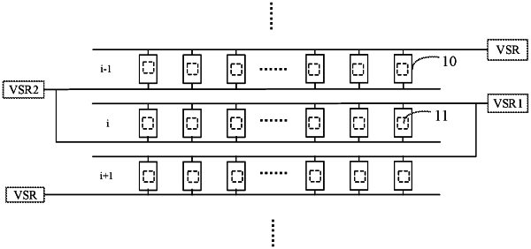
a first shift register unit connected to data writing transistors in an ith row of pixel circuits and data writing transistors in an (i+1)th row of pixel circuits, and configured to provide a first controlling signal for the two adjacent rows of pixel circuits, wherein for each of the ith and (i+1)th rows of pixel circuits, a first electrode of the respective data writing transistor is electrically connected to a data signal line, a second electrode of the respective data writing transistor is electrically connected to a first electrode of the respective threshold compensating transistor, and the respective data writing transistor is turned on in response to the first controlling signal; and
a second shift register unit connected to threshold compensating transistors in the ith row of pixel circuits and threshold compensating transistors in an (i−1)th row of pixel circuits, and configured to provide a second controlling signal for the two adjacent rows of pixel circuits, wherein for each of the ith and (i−1)th rows of pixel circuits, a first electrode of the respective threshold compensating transistor is electrically connected to a second electrode of the respective data writing transistor, a second electrode of the respective threshold compensating transistor is electrically connected to a gate of the respective driving transistor, and the respective threshold compensating transistor is turned on in response to the second controlling signal; and
wherein for each of the pixel circuits, a first turn-on period of the respective data writing transistor is partially overlapped with a second turn-on period of the respective threshold compensating transistor,
where i is a positive integer,
wherein the first turn-on period is between a falling edge and a rising edge of the first controlling signal, and the second turn-on period is between a rising edge and a falling edge of the second controlling signal; and
wherein the rising edge of the second controlling signal is before the falling edge of the first controlling signal, and the falling edge of the second controlling signal is before the rising edge of the first controlling signal; or
the rising edge of the second controlling signal is after the falling edge of the first controlling signal, and the falling edge of the second controlling signal is after the rising edge of the first controlling signal.
|