| CPC G09G 3/32 (2013.01) [G09G 3/2007 (2013.01); G09G 2300/0819 (2013.01); G09G 2300/0852 (2013.01); G09G 2300/0861 (2013.01); G09G 2310/0286 (2013.01); G09G 2310/08 (2013.01); G09G 2320/0233 (2013.01)] | 10 Claims |
|
1. A pixel drive circuit, comprising: a drive sub-circuit, a write sub-circuit and a control circuit coupled at a first node, wherein
the write sub-circuit is further coupled to a first scanning signal terminal and a first data signal terminal, and is configured to write a first data voltage from the first data signal terminal to the first node under control of a first scanning signal provided by the first scanning signal terminal;
the control circuit is further coupled to a light-emitting control signal terminal, a second scanning signal terminal and a second data signal terminal, and is configured to determine a duration of providing a driving signal to a to-be-driven element under control of a light-emitting control signal provided by the light-emitting control signal terminal and a second scanning signal provided by the second scanning signal terminal; and
the drive sub-circuit is configured to generate the driving signal for driving the to-be-driven element based on the first data voltage and a first power supply voltage supplied from the first power supply terminal,
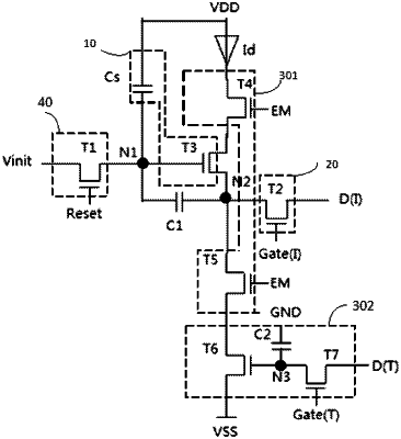
wherein the pixel drive circuit further comprises a reset voltage terminal, a reset control signal terminal, the light-emitting control signal terminal, the first data signal terminal, a second data signal terminal, the first scanning signal terminal, the second scanning signal terminal, the first power supply terminal, second and third power supply terminals, a reset sub-circuit, and a compensation sub-circuit, wherein the reset sub-circuit comprises a first transistor, the compensation sub-circuit comprises a first capacitor, the write sub-circuit comprises a second transistor, the drive sub-circuit comprises a storage capacitor and a third transistor, and the control circuit comprises fourth to seventh transistors and a second capacitor, wherein
a first electrode of the first transistor, one end of the first capacitor, a control electrode of the third transistor, and one end of the storage capacitor are coupled at a second node,
a control electrode of the first transistor is coupled to the reset control signal terminal, a second electrode of the first transistor is coupled to the reset voltage terminal,
the other end of the storage capacitor is coupled to the first power supply terminal,
the other end of the first capacitor, a second electrode of the third transistor, a first electrode of the second transistor, and a first electrode of the filth transistor are coupled at the first node,
a first electrode of the third transistor is coupled to a second electrode of the fourth transistor,
a first electrode of the fourth transistor is coupled to a first electrode of a to-be-driven element, and a control electrode of the fourth transistor is coupled to the light-emitting control signal terminal,
the other electrode of the to-be-driven element is coupled to the first power supply terminal, and
a control electrode of the second transistor is coupled to the first scanning signal terminal, and a second electrode of the second transistor is coupled to the second data signal terminal,
a control electrode of the fifth transistor is coupled to the light-emitting control signal terminal, and a second electrode of the fifth transistor is coupled to a first electrode of the sixth transistor, and
a control electrode of the sixth transistor, one end of the second capacitor, and a first electrode of the seventh transistor are coupled at a third node,
a second electrode of the sixth transistor is coupled to the second power supply terminal,
a control electrode of the seventh transistor is coupled to the second scanning signal terminal, and a second electrode of the seventh transistor is coupled to the second data signal terminal, and
the other another end of the second capacitor is coupled to the third power supply terminal.
|
|
5. A method for driving a pixel drive circuit, wherein the pixel drive circuit comprises: a drive sub-circuit, a write sub-circuit and a control circuit coupled at a first node, wherein
the write sub-circuit is further coupled to a first scanning signal terminal and a first data signal terminal, and is configured to write a first data voltage from the first data signal terminal to the first node under control of a first scanning signal provided by the first scanning signal terminal;
the control circuit is further coupled to a light-emitting control signal terminal, a second scanning signal terminal and a second data signal terminal, and is configured to determine a duration of providing a driving signal to a to-be-driven element under control of a light-emitting control signal provided by the light-emitting control signal terminal and a second scanning signal provided by the second scanning signal terminal; and
the drive sub-circuit is configured to generate the driving signal for driving the to-be-driven element based on the first data voltage and a first power supply voltage supplied from the first power supply terminal,
wherein a plurality of scanning phases arm comprised in one image frame, each of the plurality of scanning phases comprising a first scanning phase and a second scanning phase; the gray scale control circuit comprises a light-emitting control circuit and a gray scale control circuit;
and the driving method comprises: within one image frame,
providing, in a data write phase, the first scanning signal to the first scanning signal terminal, and the first data voltage to the first data signal terminal, and writing the first data voltage into the drive sub-circuit via the write sub-circuit;
providing, in the first scanning phase, the second scanning signal to the second scanning signal terminal, and a second data voltage to the second data signal terminal such that the gray scale control circuit provides a current-connection path or a current-disconnection path to the to-be-driven element under control of the second scanning signal and the second data voltage; and providing a light-emitting control signal to the light-emitting control signal terminal such that the light-emitting control circuit provides a current-connection path to the to-be-driven element under control of the light-emitting control signal; and
providing, in the second scanning phase, the second scanning signal to the second scanning signal terminal, and the second data voltage to the second data signal terminal such that the gray scale control circuit provides the current-connection path or the current-disconnection path to the to-be-driven element under control of the second scanning signal and the second data voltage; and providing the light-emitting control signal to the light-emitting control signal terminal such that the light-emitting control circuit provides the current-connection path to the to-be-driven element under control of the light-emitting control signal,
wherein in response to the second data voltage at an active level, the to-be-driven element is driven under common control of the current-connection path provided by the gray scale control circuit and the current-connection path provided by the light-emitting control circuit;
and in response to the second data voltage at an inactive level, the to-be-driven element is not driven under common control of the current-disconnection path provided by the gray scale control circuit and the current-connection path provided by the light-emitting control circuit,
wherein
the first scanning phase comprises a first data read phase and a first light-emitting phase, and the second scanning phase comprises a second data read phase and a second light-emitting phase,
in the first data read phase, the second scanning signal is provided to the second scanning signal terminal, the second data voltage at an inactive level is provided to the second data signal terminal, and the gray scale control circuit provides the current-connection path to the to-be-driven element, and
in the first light-emitting phase, the light-emitting control signal is provided to the light-emitting control signal terminal, and the light-emitting control circuit provides the current-connection path to the to-be-driven element while the gray scale control circuit provides the current-disconnection path to the to-be-driven element so that the to-be-driven element is not driven in the first light-emitting phase; and
in the second data read phase, the second scanning signal is provided to the second scanning signal terminal, the second data voltage at an active level is provided to the second data signal terminal, and the gray scale control circuit provides the current-connection path to the to-be-driven element until end of the second light-emitting phase, and
in the second light-emitting phase, the light-emitting control signal is provided to the light-emitting control signal terminal, and both the light-emitting control circuit and the gray scale control circuit provide the current-connection path to the to-be-driven element so that the to-be-driven element is driven in the second light-emitting phase.
|