| CPC G09G 3/006 (2013.01) [G09G 3/3275 (2013.01); G09G 3/3688 (2013.01); G09G 2310/0291 (2013.01); G09G 2330/04 (2013.01); G09G 2330/12 (2013.01)] | 5 Claims |
|
1. A display driver, comprising:
first to n-th amplifier circuits that receive first to n-th (n is an integer of 2 or greater) gradation voltages each having a voltage value corresponding to a luminance level of each pixel indicated by a video signal, generate first to n-th output currents that are electric currents corresponding to a size of change in voltage values of the first to n-th gradation voltages respectively, and supply first to n-th output voltages having voltage values corresponding to the first to n-th gradation voltages respectively to first to n-th source lines of a display panel by outputting the generated first to n-th output currents to the first to n-th source lines of the display panel, respectively;
a failure determination circuit that determines whether a short circuit failure or current leak failure is occurring or has occurred in the first to n-th source lines or not; and
a common wiring line connected to each of the first to n-th amplifier circuits,
wherein each of the first to n-th amplifier circuits comprises:
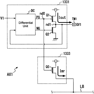
a differential unit that generates a differential signal that represents a difference between the gradation voltage and the output voltage;
a first transistor that receives the differential signal at a gate thereof, and sends out an output current from a drain thereof to the common wiring line; and
a second transistor that receives the differential signal at a gate thereof, and sends out a mirror current that is a copy of the output current sent from the first transistor to the common wiring line, and
wherein the failure determination circuit comprises:
a variable resistance that is connected to the common wiring line and that generates an output current detection signal at the common wiring line upon receiving a combined current of mirror currents sent from second transistors of respective amplifier circuits via the common wiring line; and
a comparator that determines whether a short-circuit failure or a current leak failure is occurring or has occurred in the first to n-th source lines by comparing a level of the output current detection signal with a prescribed threshold value.
|