| CPC G06V 40/13 (2022.01) [H01L 31/02016 (2013.01); H01L 31/02164 (2013.01); H01L 31/18 (2013.01)] | 19 Claims |
|
1. A method for forming a semiconductor device, comprising:
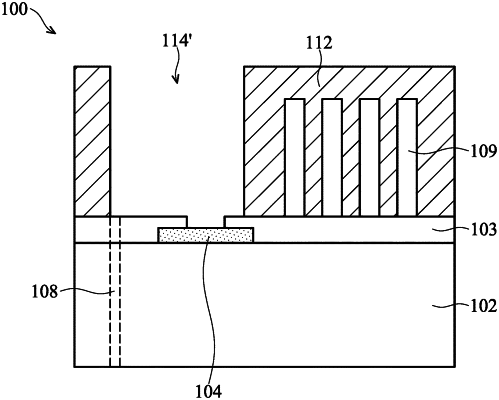
providing a substrate with a conductive pad formed thereon;
forming a transparent structure over the substrate, wherein the transparent structure comprises a plurality of collimating pillars adjacent to the conductive pad;
forming a light-shielding structure over the plurality of collimating pillars and the conductive pad, wherein the light-shielding structure is disposed between the plurality of collimating pillars and between the plurality of collimating pillars and the conductive pad;
performing a cutting process to remove one or more materials directly above the conductive pad, while leaving remaining material covering the conductive pad, wherein the one or more materials comprise a portion of the light-shielding structure; and
performing an etching process to remove the remaining material to expose the conductive pad.
|