| CPC G06K 19/0723 (2013.01) [G06K 19/0701 (2013.01); G11C 17/16 (2013.01); G11C 17/18 (2013.01)] | 17 Claims |
|
1. A low power non-volatile non-charge-based variable supply radio frequency identification (RFID) tag memory device, comprising:
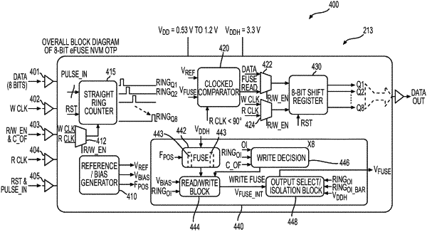
a reference/bias generator configured to receive an input voltage and to provide voltage and current for a write operation and for a read operation of the RFID tag memory device, the reference/bias generator including a first isolating component to stop high voltages during the write operation from damaging the reference/bias generator;
a clocked comparator configured to receive a reference voltage from the reference/bias generator and a voltage generated corresponding to a non-charge-based memory component voltage read from a corresponding one of a plurality of non-charge-based memory components for comparison with the reference voltage, the clocked comparator providing a non-charge-based memory component resulting value as a result of the comparison, the non-charge-based memory component resulting value corresponding to a predetermined identification (ID) value of the corresponding one of the plurality of non-charge-based memory components forming a part of a predetermined ID for the RFID tag memory device;
a shift register in communication with the clocked comparator and being configured to receive for the read operation each non-charge-based memory component resulting value as a result of the comparison by the clocked comparator of the reference voltage from the reference/bias generator and the voltage generated corresponding to the non-charge-based memory component voltage for each corresponding one of the plurality of non-charge-based memory components, each non-charge-based memory component resulting value being saved in a corresponding register of the shift register and corresponding to the predetermined ID value of a corresponding one of the plurality of non-charge-based memory components and, for the write operation the shift register being configured to receive and respectively store in a corresponding register of the shift register each predetermined ID value forming a part of the predetermined ID for the RFID tag memory device to be written to corresponding ones of the plurality of non-charge-based memory components;
a system memory component including a memory cell that includes the plurality of non-charge-based memory components, each non-charge-based memory component of the plurality of non-charge-based memory components being configured to be programmed to store the predetermined ID value of a corresponding one of the plurality of non-charge-based memory components;
a ring counter configured to provide a plurality of ring signals, each ring signal of the plurality of ring signals for sequentially respectively writing to or reading from each corresponding one of the plurality of non-charge-based memory components the predetermined ID value, the predetermined ID value written to corresponding ones of the plurality of non-charge-based memory components forming a part of the predetermined ID for the RFID tag memory device;
a read/write component associated with the system memory component, the read/write component configured to sequentially respectively receive ring signals for the write operation or ring signals for the read operation of the plurality of ring signals from the ring counter and respectively receive a read current or write current from the reference/bias generator to respectively sequentially read or write the predetermined ID value forming a part of the predetermined ID for the RFID tag memory device to or from each of corresponding ones of the plurality of non-charge-based memory components, each predetermined ID value collectively comprising the predetermined ID for ef the RFID tag memory device, the read/write component providing the voltage generated corresponding to the non-charge-based memory component voltage read from a corresponding one of the plurality of non-charge-based memory components indicating the predetermined ID value for the corresponding one of the plurality of non-charge-based memory components;
a write decision component configured to sequentially receive ring signals for the write operation of the plurality of ring signals from the ring counter to enable the write operation to respectively sequentially write the predetermined ID value to each of corresponding ones of the plurality of non-charge-based memory components forming a part of the predetermined ID for the RFID tag memory device, the write decision component being disabled during the read operation of reading the predetermined ID value written to each of corresponding ones of the plurality of non-charge-based memory components; and
an output select/isolation component configured to sequentially receive ring signals for the read operation of the plurality of rings signals from the ring counter and the voltage generated from the read/write component corresponding to the non-charge based memory component voltage reader from a corresponding one of the plurality of non-charge-based memory component indicating a corresponding predetermined ID value the output select/isolation component providing the voltage generated to the clocked comparator for the comparison with the received reference voltage, the output select/isolation component in communication with a second isolating component to isolate a high writing voltage during the write operation from being provided to the clocked comparator.
|