| CPC G06F 7/588 (2013.01) [G11C 11/412 (2013.01); G11C 11/419 (2013.01); H01L 27/088 (2013.01); H03K 3/037 (2013.01); H03K 3/84 (2013.01)] | 7 Claims |
|
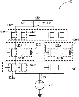
1. A random number generator comprising:
a voltage source configured to provide a scan voltage during enroll operations;
a first select circuit coupled to a first main bit line and a second main bit line;
a second select circuit coupled to the voltage source;
a plurality of bit data cells, each comprising:
a first transistor having a first terminal coupled to the first select circuit, a second terminal coupled to the second select circuit, and a control terminal; and
a second transistor having a first terminal coupled to the first select circuit, a second terminal coupled to the second select circuit, and a control terminal; and
a sensing control circuit coupled to the first select circuit through the first main bit line and the second main bit line;
wherein during an enroll operation of a first bit data cell of the plurality of bit data cells:
the first select circuit forms an electrical connection between the first main bit line and the first bit data cell, and forms an electrical connection between the second main bit line and the first bit data cell;
the second select circuit forms electrical connections between the voltage source and the first bit data cell; and
the sensing control circuit outputs a random bit based on a punch through current of the first transistor or a punch through current of the second transistor;
wherein the scan voltage provided by the voltage source induces the punch through current of the first transistor or the punch through current of the second transistor.
|