| CPC G06F 30/392 (2020.01) [G06F 17/16 (2013.01); G06N 3/063 (2013.01); G11B 5/09 (2013.01); G11B 5/3146 (2013.01); G11C 11/418 (2013.01); G11C 11/54 (2013.01); H01L 27/0924 (2013.01); H10B 10/12 (2023.02); H10B 10/18 (2023.02)] | 20 Claims |
|
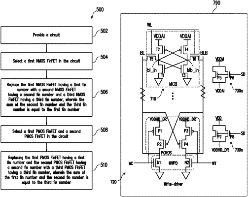
1. A method of designing a circuit, comprising:
providing a circuit including a write driver comprising:
a first PMOS FinFET having a first source/drain terminal coupled to a first power terminal;
a second PMOS FinFET having a first source/drain terminal coupled to a second source/drain terminal of the first PMOS FinFET, and a gate terminal coupled to a first bit line;
a third PMOS FinFET having a first source/drain terminal coupled to the first power terminal;
a fourth PMOS FinFET having a first source/drain terminal coupled to a second source/drain terminal of the third PMOS FinFET, and a gate terminal coupled to a second bit line;
a first NMOS FinFET connected between a second source/drain terminal of the second PMOS FinFET and a second power terminal wherein gate terminal of the first NMOS FinFET is connected to a first write input terminal; and
a fourth NMOS FinFET connected between a second source/drain terminal of the fourth PMOS FinFET and a second power terminal, wherein a gate terminal of the fourth NMOS FinFET is connected to a second write input terminal;
determining a first number of fins for the first NMOS FinFET in the circuit based on a first criterion;
modifying the circuit by replacing the first NMOS FinFET having the first number of fins with a second NMOS FinFET having a second number of fins and a third NMOS FinFET having a third number of fins based on a second criterion, wherein the sum of the second number of fins and the third number of fins is equal to the first number of fins; and
generating a circuit design layout based on the modified circuit.
|