| CPC G06F 30/392 (2020.01) [G06F 30/398 (2020.01); H01L 27/0207 (2013.01); G06F 2111/04 (2020.01)] | 11 Claims |
|
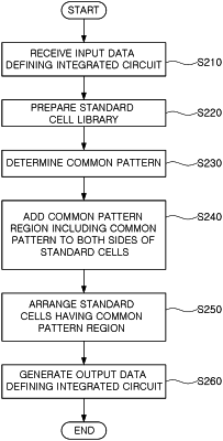
1. A method of designing a layout of a semiconductor device, comprising:
preparing a standard cell library comprising information on standard cells;
determining a common active pattern in consideration of a local layout effect based on the standard cell library;
adding a common pattern region comprising the common active pattern to opposite sides of the standard cells, respectively; and
arranging the standard cells comprising the common pattern region,
wherein the standard cells comprise a first standard cell and a second standard cell that are adjacent to each other,
wherein, in the arranging the standard cells,
responsive to a width of the common active pattern being identical to a width of active patterns in the first and second standard cells, the common pattern region is arranged to overlap the first and second standard cells, and
responsive to the width of the common active pattern being different from the width of the active patterns in at least one of the first standard cell or the second standard cell, the common pattern region is arranged to be shared between the first and second standard cells.
|