| CPC G06F 3/0659 (2013.01) [G06F 3/0604 (2013.01); G06F 3/0653 (2013.01); G06F 3/0673 (2013.01); G11C 29/10 (2013.01); G11C 29/56004 (2013.01)] | 20 Claims |
|
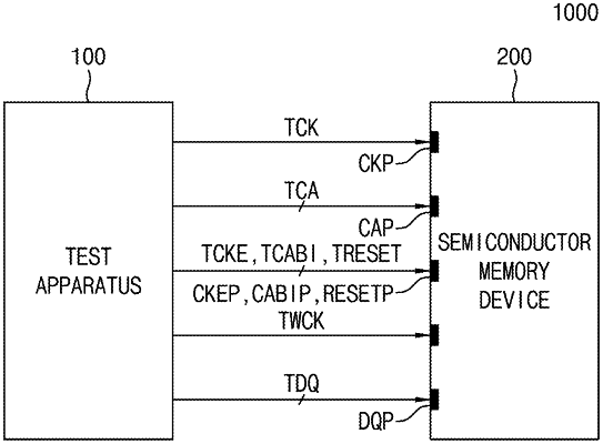
1. A semiconductor memory device comprising:
a memory cell array including a plurality of memory cells storing data;
a command/address generation circuit configured to generate a test read command and a test pattern data selection signal in response to receiving a test clock signal;
a test pattern data storage including a plurality of registers, each of the plurality of registers storing m-bit test pattern data, and configured to select first m-bit test pattern data from one of the plurality of registers in response to receiving the test read command and the test pattern data selection signal, wherein m is a natural number greater than 1;
a read path circuit configured to read stored m-bit data from the memory cell array; and
a test read data generation circuit configured to compare the first m-bit test pattern data and the m-bit data, and generate n-bit test data based on a comparison of the first m-bit test pattern data and the m-bit data, wherein n is a natural number greater than 1.
|