| CPC G06F 3/0655 (2013.01) [G06F 3/0604 (2013.01); G06F 3/0679 (2013.01); G11C 7/1048 (2013.01); G11C 7/1066 (2013.01); G11C 7/1093 (2013.01); G11C 7/222 (2013.01); G11C 16/0483 (2013.01); G11C 16/10 (2013.01); G11C 16/32 (2013.01); H03G 3/3036 (2013.01); H04L 7/0079 (2013.01)] | 20 Claims |

|
1. A semiconductor integrated circuit comprising:
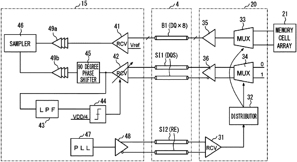
a reception circuit configured to receive a strobe signal of which a logic is intermittently switched in synchronization with a data signal and change a boost amount of at least a high frequency component of the received strobe signal;
an output circuit configured to extract a low frequency component including at least a DC component of the strobe signal received by the reception circuit and to output a first signal; and
a comparison circuit configured to compare a signal level of the first signal with a threshold level,
wherein the reception circuit is configured to change the boost amount of at least the high frequency component of the strobe signal based on a comparison result obtained by the comparison circuit.
|