| CPC G06F 3/0619 (2013.01) [G06F 3/0659 (2013.01); G06F 3/0673 (2013.01)] | 20 Claims |
|
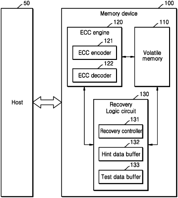
1. A memory device comprising:
a volatile memory comprising a plurality of memory cells, a plurality of word lines and a plurality of bit lines, and configured to provide output data stored in target memory cells, among the plurality of memory cells, based on a first read command and an address received from a host;
a recovery logic circuit configured to provide hint data indicating first bit lines to which defective cells are connected, and second bit lines to which other cells are connected, among the plurality of bit lines;
an Error Correction Circuit (ECC) configured to generate corrected data by correcting an error in the output data based on the output data and the hint data, and to provide the corrected data to the host; and
a recovery controller configured to control the volatile memory to store first test pattern data in the target memory cells, control the volatile memory to read first test data from the target memory cells, control the volatile memory to store second test pattern data in the target memory cells, control the volatile memory to read second test data from the target memory cells, and generate the hint data based on the first test data and the second test data.
|