| CPC G06F 3/0611 (2013.01) [G06F 3/0629 (2013.01); G06F 3/0673 (2013.01)] | 20 Claims |
|
1. A memory system, comprising:
a main memory comprising:
a first plurality of input/outputs (I/Os) configured to output data stored in the main memory in response to a read access request having a corresponding access address, wherein a first portion of the first plurality of IOs is configured to provide user read data in response to the read access request and a second portion of the first plurality of IOs is configured to provide candidate replacement IOs; and
repair circuitry configured to selectively replace one or more IOs of the first portion of the first plurality of IOs using one or more of the candidate replacement IOs of the second portion of the first plurality of IOs to provide repaired read data in response to the read access request in accordance with repair mapping information corresponding to the corresponding access address;
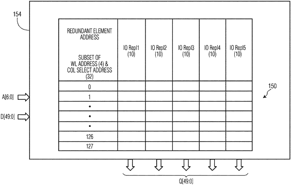
a static random access memory (SRAM) separate from the main memory and configured to store repair mapping information corresponding to address locations of the main memory; and
a repair cache configured to store cached repair mapping information from the SRAM for one or more address locations of the main memory, wherein the SRAM is a backing store for the repair cache.
|