| CPC G06F 3/0448 (2019.05) [G06F 3/0412 (2013.01); H10K 59/122 (2023.02); H10K 59/40 (2023.02); G06F 2203/04112 (2013.01)] | 20 Claims |
|
1. A display device comprising:
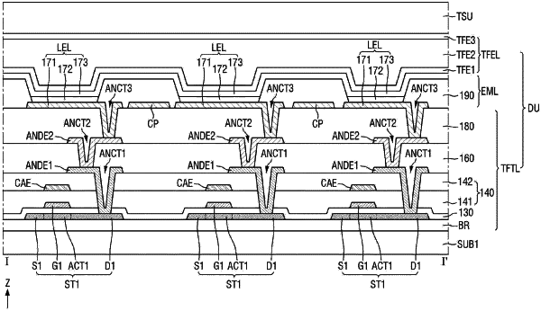
a plurality of unit pixels on a substrate, wherein each unit pixel of the plurality of unit pixels includes a plurality of subpixels;
a plurality of position code patterns having a predetermined position code shape, wherein, when viewed in a plan view, each position code pattern of the plurality of position code patterns is disposed at a region between at least two adjacent subpixels among the plurality of subpixels; and
a pixel-defining layer covering the plurality of position code patterns and defining a region where each subpixel of the plurality of subpixels is disposed,
wherein the plurality of position code patterns are formed in a planar code shape and are configured to reflect light incident through the pixel-defining layer,
wherein each subpixel of the plurality of subpixels includes a light-emitting element, which includes a pixel electrode, an emission layer, and a common electrode,
wherein, when viewed in a plan view, each position code pattern of the plurality of position code patterns is disposed at a corresponding unit pixel of the plurality of unit pixels and is disposed between at least two adjacent pixel electrodes of a plurality of pixel electrodes in the corresponding unit pixel,
wherein, when viewed in the plan view, each position code pattern is spaced apart from the at least two adjacent pixel electrodes in the corresponding unit pixel, and
wherein the plurality of position code patterns are formed and disposed on the same layer as the plurality of pixel electrodes using the same metal material as the plurality of pixel electrodes.
|