| CPC G06F 13/42 (2013.01) [G06F 1/06 (2013.01); G06F 1/08 (2013.01); H03K 3/037 (2013.01)] | 16 Claims |
|
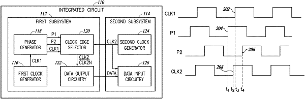
1. A method, comprising:
generating a first clock signal with a first subsystem of an integrated circuit;
generating a second clock signal with a second subsystem of the integrated circuit;
determining a phase difference between the first clock signal and the second clock signal; and
selecting an edge of the second clock signal based on the phase difference;
controlling transmission of data from the first subsystem to the second subsystem with the selected edge of the second clock signal;
generating, with the first subsystem, a first phase signal having a same frequency as the first clock signal and a first selected phase difference relative to the first clock signal; and
generating, with the first subsystem, a second phase signal having the same frequency as the first clock signal and a second selected phase difference relative to the first clock signal.
|