| CPC G06F 13/362 (2013.01) [G06F 13/4031 (2013.01); G06F 13/404 (2013.01); G06F 13/4045 (2013.01)] | 20 Claims |
|
1. A method, comprising:
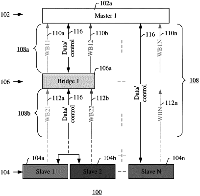
routing a write transaction from a master device to a slave device through a communication path, the communication path including a first bridge and a second bridge downstream of the first bridge, wherein the first bridge and the second bridge are coupled to one another via an interface structure,
wherein the first bridge sets a write busy signal on the communication path when the write transaction is processed by the first bridge; and in response to the first bridge setting the write busy signal, the second bridge holds the write busy signal set until the write transaction has been received by the slave device;
upon the slave device receiving the write transaction, the second bridge resets the write busy signal to propagate the reset write busy signal back to the master device through the first bridge;
providing a write ready signal from the first bridge when the first bridge is ready to receive data from the master device; and
triggering a synchronization event when the master device receives the write ready signal.
|