| CPC G06F 13/12 (2013.01) [G06F 13/1668 (2013.01); G11C 11/221 (2013.01); G11C 11/2259 (2013.01); G11C 11/4093 (2013.01); G11C 11/2273 (2013.01); G11C 11/4091 (2013.01)] | 20 Claims |
|
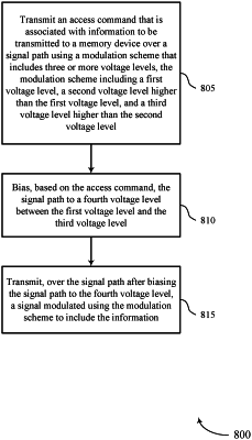
1. A method, comprising:
transmitting an access command that is associated with information to be transmitted to a memory device over a signal path using a modulation scheme that includes three or more voltage levels, the three or more voltage levels comprising a first voltage level, a second voltage level higher than the first voltage level, and a third voltage level higher than the second voltage level;
biasing, based at least in part on the access command, the signal path to a fourth voltage level between the first voltage level and the third voltage level; and
transmitting, over the signal path after biasing the signal path to the fourth voltage level, a signal modulated using the modulation scheme to include the information.
|