| CPC G06F 12/0862 (2013.01) [G06F 3/0611 (2013.01); G06F 3/0659 (2013.01); G06F 3/0673 (2013.01); G06F 2212/305 (2013.01); G06F 2212/6022 (2013.01)] | 15 Claims |
|
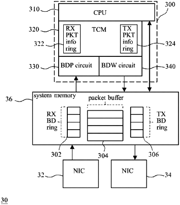
1. A device for packet processing acceleration comprising a central processing unit (CPU), a tightly coupled memory (TCM), a buffer descriptor (BD) prefetch circuit, and a BD write back circuit, wherein:
the TCM is coupled to the CPU;
the BD prefetch (BDP) circuit is coupled to the TCM, and configured to read multiple pieces of reception-end (RX) BD data stored in an RX BD ring according to a BD extraction map and then write the multiple pieces of RX BD data into an RX packet information ring; and the BDP circuit is further configured to read multiple pieces of RX header data stored in a packet buffer according to a buffer extraction map, and then write the multiple pieces of RX header data into the RX packet information ring, wherein both the RX BD ring and the packet buffer are included in a system memory and the RX packet information ring is included in the TCM;
the CPU is configured to access the RX packet information ring to read and process the multiple pieces of RX BD data and the multiple pieces of RX header data and thereby generate multiple pieces of transmission-end (TX) BD data and multiple pieces of TX header data; and the CPU is further configured to write the multiple pieces of TX BD data and the multiple pieces of TX header data into a TX packet information ring, wherein the TX packet information ring is included in the TCM; and
the BD write back (BDW) circuit is coupled to the TCM, and configured to read the multiple pieces of TX BD data stored in the TX packet information ring and then write the multiple pieces of TX BD data into a TX BD ring; and the BDW circuit is further configured to read the multiple pieces of TX header data stored in the TX packet information ring and then write the multiple pieces of TX header data into the packet buffer, wherein the TX BD ring is included in the system memory.
|