| CPC G06F 11/2094 (2013.01) [G06F 12/0875 (2013.01); G06F 12/10 (2013.01); G11C 11/4091 (2013.01); G11C 29/4401 (2013.01); G06F 2201/82 (2013.01); G06F 2212/45 (2013.01); G11C 11/4085 (2013.01)] | 20 Claims |
|
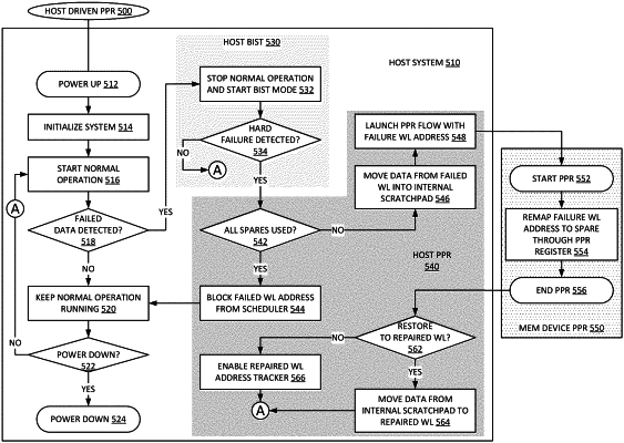
1. A memory device comprising:
a memory array having multiple rows of memory, including a failure row detected to have a failure;
an internal scratchpad memory internal to the memory device; and
an internal controller of the memory device to receive an address of the failure row from a host controller, the internal controller to execute a post package repair (PPR) mode, including:
map a logical address of the failure row from a physical address of the failure row to a physical address of a spare row,
transfer data contents from the failure row to the internal scratchpad memory without transferring the data contents to the host controller, and
transfer the data contents from the internal scratchpad memory to the spare row.
|