| CPC G06F 1/08 (2013.01) [H03B 5/1228 (2013.01); H03L 7/0991 (2013.01); H03L 7/187 (2013.01)] | 14 Claims |
|
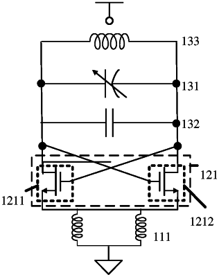
1. An oscillator comprising:
a resonant circuit having first and second ends;
a first tail inductance comprising at least two first inductors connected in parallel to a power supply or a ground;
a first transistor and a second transistor that are cross-coupled, wherein sources of the first transistor and the second transistor are connected together and are connected to the power supply or the ground through the first tail inductance,
a gate of the first transistor, a drain of the second transistor, and the first end of the resonant circuit are coupled to a first node,
a drain of the first transistor, a gate of the second transistor, and the second end of the resonant circuit are coupled to a second node;
a second tail inductance comprising at least two second inductors connected in parallel;
a third transistor and a fourth transistor that are cross-coupled, and sources of the third transistor and the fourth transistor being coupled to the ground through the second tail inductance; and
a gate of the third transistor and a drain of the fourth transistor are coupled to the first node, and a drain of the third transistor and a gate of the fourth transistor are coupled to the second node.
|