| CPC G05F 1/575 (2013.01) [G05F 1/565 (2013.01)] | 20 Claims |
|
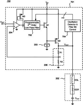
1. A low drop-out (LDO) regulator circuit configured to be coupled to a capacitive load, the LDO regulator circuit including:
(a) a pass field-effect transistor (FET) including a control gate and configured to produce a voltage output from an input voltage;
(b) a driver FET including a control gate and configured to provide a control voltage to the control gate of the pass FET;
(c) a feedback loop coupled between the voltage output and an internal node;
(d) a low pass filter (LPF) coupled between the internal node and the control gate of the driver FET and settable to one of a plurality of tuning states in response to application of an N-bit binary signal to the LPF; and
(e) an oscillation detector and filter bit control circuit, coupled to a voltage output of the LDO regulator circuit and to the LPF, and configured to detect an oscillation in the voltage output of the LDO regulator circuit and to generate a filter bit pattern as the N-bit binary signal as a function of the detected oscillation, wherein the N-bit binary signal selects one of the plurality of tuning states of the LPF to at least partially control the oscillation in the voltage output of the LDO regulator circuit.
|