| CPC G03G 15/5037 (2013.01) [G03G 15/0266 (2013.01); G03G 15/55 (2013.01)] | 17 Claims |
|
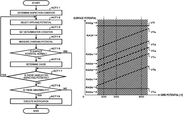
9. A method for an image forming apparatus, comprising:
detecting an actual charging potential of a photoconductor by a charger after the photoconductor is charged by the charger; and
determining one of a plurality of causes related to a charging abnormality of the photoconductor based on a relationship between a standard charging potential of the photoconductor obtained by charging by the charger and a charging potential detected;
charging the photoconductor with a plurality of different charging amounts and allowing detection of the actual charging potential of the photoconductor after the photoconductor is charged with the plurality of different charging amounts; and
determining one of the plurality of causes related to the charging abnormality of the photoconductor based on a relationship between the standard charging potential of the photoconductor to be obtained by charging with a certain charging amount and the charging potential detected with respect to the photoconductor charged with the charging amount in relation to each of the plurality of charging amounts.
|