US 11,988,972 B2
Method and apparatus for improving critical dimension variation
Ming-Hsun Lin, Hsinchu (TW); Yu-Hsiang Ho, Hsinchu (TW); Jhun Hua Chen, Changhua (TW); Chi-Hung Liao, Sanchong (TW); and Teng Kuei Chuang, Taichung (TW)
Assigned to TAIWAN SEMICONDUCTOR MANUFACTURING COMPANY, LTD., Hsinchu (TW)
Filed by TAIWAN SEMICONDUCTOR MANUFACTURING COMPANY, LTD., Hsinchu (TW)
Filed on Feb. 13, 2023, as Appl. No. 18/109,183.
Application 18/109,183 is a continuation of application No. 17/380,633, filed on Jul. 20, 2021, granted, now 11,579,539.
Claims priority of provisional application 63/156,016, filed on Mar. 3, 2021.
Prior Publication US 2023/0195000 A1, Jun. 22, 2023
This patent is subject to a terminal disclaimer.
Int. Cl. G03F 7/00 (2006.01)
CPC G03F 7/7085 (2013.01) [G03F 7/70558 (2013.01); G03F 7/70925 (2013.01)] 20 Claims
OG exemplary drawing
 
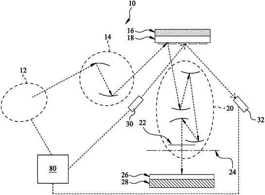
1. A method, comprising:
obtaining a relationship between thicknesses of a contamination layer formed on a mask and amounts of compensation energy to remove the contamination layer;
measuring a first thickness of a first contamination layer formed on the mask; and
increasing an energy applied to a first light from a first light source to the mask multiple times to remove the first contamination layer, wherein each time an amount of increase in the energy is less than an amount of increase in the energy in the previous time.