| CPC G03F 7/70633 (2013.01) [G06T 7/0004 (2013.01); H01L 22/20 (2013.01); G06T 2207/30148 (2013.01)] | 18 Claims |
|
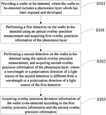
1. A method for detecting an overlay precision, comprising:
providing a wafer to-be-detected, wherein the wafer to-be-detected includes a photoresist layer which has been exposed and developed;
performing a first detection on the wafer to-be-detected using an optical overlay precision measurement and acquiring first overlay precision information of the photoresist layer, the optical overlay precision measurement including an overlay precision measurement based on imaging and image recognition;
performing a second detection on the wafer to-be-detected using the optical overlay precision measurement, and acquiring second overlay precision information of the photoresist layer, wherein a wavelength or a polarization direction of a light source of the second detection is different from a wavelength or a polarization direction of a light source of the first detection; and
acquiring overlay precision deviation information of the wafer to-be-detected according to the first overlay precision information and the second overlay precision information.
|