US 11,988,961 B2
Radiation based patterning methods
Jason K. Stowers, Corvallis, OR (US); Alan J. Telecky, Albany, OR (US); Douglas A. Keszler, Corvallis, OR (US); and Andrew Grenville, Corvallis, OR (US)
Assigned to Inpria Corporation, Corvallis, OR (US)
Filed by Inpria Corporation, Corvallis, OR (US)
Filed on May 22, 2023, as Appl. No. 18/200,125.
Application 15/784,258 is a division of application No. 14/858,612, filed on Sep. 18, 2015, granted, now 9,823,564, issued on Nov. 21, 2017.
Application 18/200,125 is a continuation of application No. 17/895,657, filed on Aug. 25, 2022, granted, now 11,693,312.
Application 17/895,657 is a continuation of application No. 17/839,784, filed on Jun. 14, 2022, granted, now 11,599,022, issued on Mar. 7, 2023.
Application 17/839,784 is a continuation of application No. 16/885,581, filed on May 28, 2020, granted, now 11,392,031, issued on Jul. 19, 2022.
Application 16/885,581 is a continuation of application No. 15/784,258, filed on Oct. 16, 2017, granted, now 10,782,610, issued on Sep. 22, 2020.
Application 14/858,612 is a continuation of application No. 12/850,867, filed on Aug. 5, 2010, granted, now 9,176,377, issued on Nov. 3, 2015.
Claims priority of provisional application 61/350,103, filed on Jun. 1, 2010.
Prior Publication US 2023/0305390 A1, Sep. 28, 2023
This patent is subject to a terminal disclaimer.
Int. Cl. G03F 7/004 (2006.01); G03F 7/20 (2006.01); G03F 7/32 (2006.01)
CPC G03F 7/0043 (2013.01) [G03F 7/0042 (2013.01); G03F 7/20 (2013.01); G03F 7/327 (2013.01); Y10T 428/24355 (2015.01)] 21 Claims
OG exemplary drawing
 
1. A method of making a device, the method comprising:
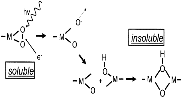
A) irradiating along a pattern, a layer of a coating material comprising metal ions with radiation sensitive ligands on the surface of a underlying structure, with EUV radiation to form a coating material with a latent image having irradiated coating material and un-irradiated coating material according to the pattern;
B) developing the coating material with the latent image to remove the un-irradiated coating material to form a developed patterned coating material having openings to the underlying structure;
C) depositing a deposited material through the openings to the underlying structure or etching the underlying structure through the openings; and
D) repeating steps A)-C) one or more times to form a structure for a device comprising semiconductor, dielectric, and/or electrical conductor features with a desired functionality.