| CPC G02F 1/2257 (2013.01) [G02F 1/0027 (2013.01); G02F 1/025 (2013.01); G02F 1/035 (2013.01); G02B 2006/12097 (2013.01); G02B 6/136 (2013.01); G02F 2201/122 (2013.01)] | 17 Claims |
|
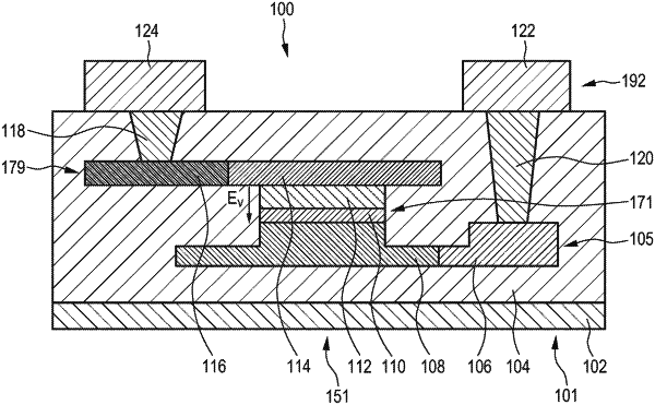
1. A method for producing an electro-optical phase shifter, comprising the steps:
providing a conducting bottom layer with a first refractive index,
providing a center layer including a ferroelectric material and with a second refractive index on top of a first region of the conducting bottom layer, such that the center layer is not on top of a second region of the conducting bottom layer, and
providing a conducting top layer with a third refractive index on top of the center layer,
wherein the second refractive index is lower than the first refractive index and lower than the third refractive index, such that the conducting bottom layer, the center layer, and the conducting top layer form a slot waveguide, such that field confinement is achieved between the conducting bottom layer and the conducting top layer, and
providing a first electrical connector which connects the second region of the conducting bottom layer with an upper layer and a second electrical connector which connects the conducting top layer with the upper layer, and
providing a first electrode and a second electrode in the upper layer such that the first electrode connects to the second region of the conducting bottom layer via the first electrical connector and the second electrode connects to the conducting top layer via the second electrical connector.
|