| CPC G02F 1/2257 (2013.01) [G02B 6/29338 (2013.01); G02B 6/2938 (2013.01); G02B 6/29395 (2013.01); G02F 1/025 (2013.01); G02F 1/3509 (2021.01); G02F 2201/17 (2013.01); G02F 2203/05 (2013.01); G02F 2203/07 (2013.01); G02F 2203/15 (2013.01)] | 20 Claims |
|
1. An optical device comprising:
a substrate;
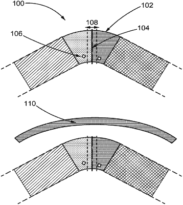
a first waveguide on the substrate that forms a ring resonator for an optical wave having a wavelength that is a specified resonant wavelength for the ring resonator, the ring resonator having a first radius of curvature to an inner edge of the first waveguide and a second radius of curvature to an outer edge of the first waveguide, wherein the first waveguide is formed from semiconductor material and has a width that supports multiple transverse optical modes at the wavelength entirely around the ring resonator;
a plurality of semiconductor junctions formed in the first waveguide that extend in a radial direction between the inner edge and the outer edge of the first waveguide, wherein each semiconductor junction of the plurality of semiconductor junctions comprises the semiconductor material having a first conductivity type on a first side of each semiconductor junction and the semiconductor material having a second conductivity type on a second side of each semiconductor junction and wherein an interfacial area between the semiconductor material having the first conductivity type and the semiconductor material having the second conductivity type extends from a lower edge to an upper edge of the first waveguide; and
a plurality of electrical contacts located radially inward from a midpoint of the first waveguide that is one-half way between the inner edge and the outer edge of the first waveguide, wherein the plurality of electrical contacts comprises a plurality of first electrical contacts that connect to the semiconductor material on the first sides of each semiconductor junction and a plurality of second electrical contacts that connect to the semiconductor material on the second sides of each semiconductor junction of the plurality of semiconductor junctions, and wherein all of the first electrical contacts and the second electrical contacts are distributed along the first waveguide and located radially inward from the midpoint of the first waveguide.
|