| CPC G02F 1/13718 (2013.01) [G02F 1/133531 (2021.01); G02F 1/13725 (2013.01)] | 17 Claims |

|
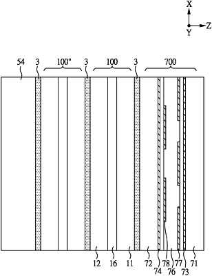
1. An electronic device, comprising:
a first light modulation assembly, comprising:
a first substrate;
a second substrate opposite to the first substrate;
a first conductive layer disposed on the first substrate;
a second conductive layer disposed on the second substrate;
a first insulating layer disposed on the first substrate; and
a first light modulation layer disposed between the first conductive layer and the second conductive layer; and
a second light modulation assembly opposite to the first light modulation assembly, wherein the second light modulation assembly comprises:
a third substrate;
a fourth substrate opposite to the third substrate;
a third conductive layer disposed on the third substrate;
a fourth conductive layer disposed on the fourth substrate;
a third insulating layer disposed on the third substrate; and
a second light modulation layer disposed between the third conductive layer and the fourth conductive layer;
a fifth conductive layer disposed on the third substrate, wherein the third insulating layer is disposed between the third conductive layer and the fifth conductive layer;
a sixth conductive layer disposed on the fourth substrate; and
a fourth insulating layer disposed on the fourth substrate, wherein the fourth insulating layer is disposed between the fourth conductive layer and the sixth conductive layer,
wherein the fifth conductive layer and the sixth conducive layer are at least partially overlapped in a top view direction.
|