| CPC G02F 1/136295 (2021.01) [G02F 1/136209 (2013.01); G02F 1/136222 (2021.01)] | 15 Claims |
|
1. A display module, comprising
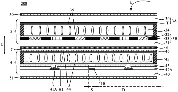
a display panel having a plurality of pixel regions; and
a dimming panel stacked on the display panel and having a plurality of dimming regions, a dimming region covering at least one pixel region in a direction perpendicular to the display panel;
wherein the dimming panel includes:
a plurality of dimming electrodes each located in a dimming region in the plurality of dimming regions, any two adjacent dimming electrodes having a gap therebetween; and
a plurality of signal lines, wherein each dimming electrode is directly electrically connected to at least one signal line; the at least one signal line is configured to transmit a control voltage signal to the dimming electrode electrically connected to the at least one signal line for controlling a light transmittance of the dimming region where the dimming electrode is located;
wherein the plurality of dimming electrodes are arranged in an array; and
a row direction in which the plurality of dimming electrodes are arranged is a first direction; and
a column direction in which the plurality of dimming electrodes are arranged is a second direction;
each signal line extends as a whole in the second direction, and the plurality of signal lines are arranged side by side in the first direction;
an orthographic projection of each signal line on the display panel is at least partially overlapped with an orthographic projection, on the display panel, of a column of dimming electrodes where a corresponding dimming electrode to which the signal line is electrically connected is located;
the signal line includes a plurality of portions connected in sequence, and is in a shape of a broken line; and every two adjacent portions constitute a bending unit; and
in the direction perpendicular to the display panel, the dimming electrode covers at least three bending units in the at least one signal line; and
the dimming panel further includes a first passivation layer disposed between the plurality of dimming electrodes and the plurality of signal lines, wherein the first passivation layer has a plurality of first vias, and each signal line is electrically connected to a corresponding dimming electrode through at least one first via.
|