| CPC G02F 1/136259 (2013.01) [H01L 27/1222 (2013.01); H01L 27/1244 (2013.01); H01L 27/1288 (2013.01); H01L 29/78669 (2013.01); G02F 1/133345 (2013.01); G02F 1/136263 (2021.01)] | 17 Claims |
|
10. An electronic display device having a multi-layer interconnection structure, comprising:
a foundation layer;
a plurality of pixels provided in corresponding pixel parts, each pixel having at least one thin film transistor, provided on said foundation layer;
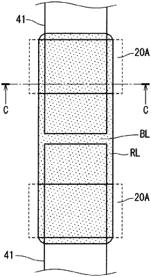
at least two conductive interconnect lines provided on said foundation layer and formed by depositing a conductor layer and etching the conductor layer, said interconnect lines each having a longitudinally extending part and an end part, said interconnect lines being electrically isolated from each other at least at one end part of each interconnect line by having a gap between adjacent end parts of the respective interconnect lines, the gap being formed at a level of the conductor layer;
an insulation film formed on said foundation layer and said interconnect lines, the insulation film also being present in the gap between the adjacent end parts of the respective interconnect lines;
a plurality of holes, each hole formed in the insulation film near a respective end part of each interconnect line that is closest to the gap between the adjacent end parts; and
a conductive film deposited at least in each hole, and above the insulation film between the ends of the interconnect lines, thereby electrically connecting the two interconnect lines, wherein at least one of the at least two interconnect lines extends to connect to a TFT terminal, further wherein in plan view, a width of each hole on an end part in a direction orthogonal to the longitudinal direction of the respective extending part of each interconnect line is at least as wide as the width of the respective extending part of each interconnect line.
|