| CPC G02F 1/136213 (2013.01) [G02F 1/13624 (2013.01); G02F 1/1368 (2013.01); H01L 27/1255 (2013.01)] | 9 Claims |
|
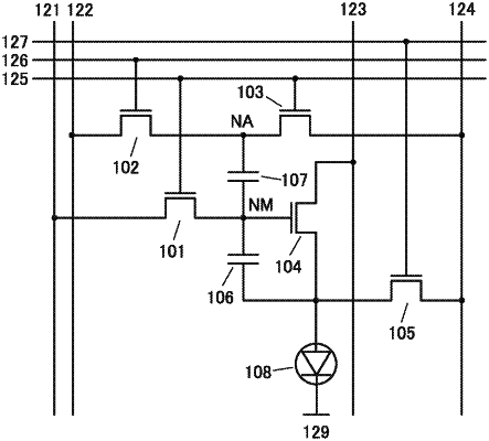
1. A display apparatus comprising, in a pixel, a first capacitor, a second capacitor, and a display element,
wherein the first capacitor and the second capacitor are electrically connected to the display element,
wherein the first capacitor comprises a structure in which a first conductive layer, a first dielectric layer, and a second conductive layer are stacked in this order,
wherein the second capacitor comprises a structure in which the second conductive layer, a second dielectric layer, and a third conductive layer are stacked in this order,
wherein the first capacitor and the second capacitor comprise a region where the first capacitor and the second capacitor overlap with each other,
wherein a potential of the first conductive layer is configured to be different from a potential of the third conductive layer,
wherein the pixel further comprises a first transistor, a second transistor, and a third transistor,
wherein one of a source and a drain of the first transistor is electrically connected to the second conductive layer, and
wherein one of a source and a drain of the second transistor and one of a source and a drain of the third transistor are electrically connected to the third conductive layer.
|