| CPC G02F 1/1345 (2013.01) | 13 Claims |
|
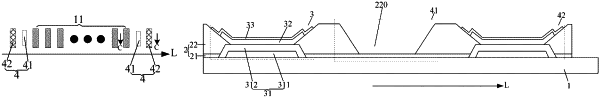
1. A driving backplate comprising a base substrate, and an insulation layer and a plurality of conductive structures on the base substrate, the insulation layer insulating the plurality of conductive structures from each other, wherein
each of the plurality of conductive structures comprises a first conductive layer and a second conductive layer stacked sequentially along a direction away from the base substrate, and at least one portion of a region in which the first conductive layer is in contact with the second conductive layer comprises a flat contact region,
an opening is at a position of the insulation layer corresponding to the conductive structure, an edge of the opening in the insulation layer is between the first conductive layer and the second conductive layer and is correspondingly in edge regions of the first conductive layer and the second conductive layer, and
an orthographic projection of the opening on the base substrate overlaps an orthographic projection, on the base substrate, of the flat contact region where the first conductive layer is in contact with the second conductive layer,
the plurality of conductive structures are arranged at intervals along a straight line direction in a non-display region, with the conductive structures at both ends of the plurality of conductive structures along the straight line direction being floating,
the insulation layer comprises a first film layer and a second film layer stacked sequentially away from the base substrate,
the driving backplate further comprises a dummy bonding terminal, the dummy bonding terminal being between the floated conductive structure at the end of the plurality of conductive structures and the remaining conductive structures and comprising a first opening in the second film layer of the insulation layer and the first film layer of the insulation layer exposed in the first opening.
|
|
10. A method for manufacturing a driving backplate, comprising:
forming an insulation layer and a plurality of conductive structures on a base substrate; the insulation layer insulating the plurality of conductive structures from each other;
forming the plurality of conductive structures comprises sequentially forming a first conductive layer and a second conductive layer, such that the first conductive layer and the second conductive layer are stacked along a direction away from the base substrate, and at least one portion of a region in which the first conductive layer is in contact with the second conductive layer comprises a flat contact region;
forming the insulation layer comprises forming an opening at a position of the insulation layer corresponding to the conductive structure, such that an edge of the opening in the insulation layer is located between the first conductive layer and the second conductive layer and is correspondingly in edge regions of the first conductive layer and the second conductive layer; wherein
an orthographic projection of the opening on the base substrate overlaps an orthographic projection, on the base substrate, of the flat contact region in which the first conductive layer is in contact with the second conductive layer,
the plurality of conductive structures are arranged at intervals along a straight line direction in a non-display region, with the conductive structures at both ends of the plurality of conductive structures along the straight line direction being floating,
forming the insulation layer further comprises forming a first film layer and a second film layer stacked sequentially away from the base substrate,
the method further comprises forming a dummy bonding terminal such that the dummy bonding terminal is between the floated conductive structure at the end of the plurality of conductive structures and the remaining conductive structures and comprises a first opening in the second film layer of the insulation layer and the first film layer of the insulation layer exposed in the first opening.
|