| CPC G02F 1/133614 (2021.01) [G02F 1/133512 (2013.01); G02F 1/133603 (2013.01); G02F 1/133528 (2013.01); G02F 2202/36 (2013.01)] | 19 Claims |
|
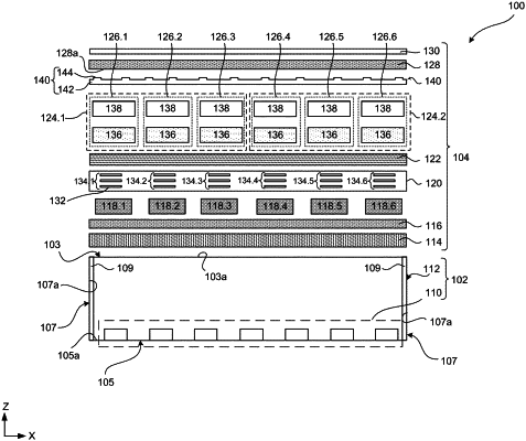
1. A display device comprising:
a backlight unit comprising a light source; and
a liquid crystal display (LCD) module comprising:
a nanostructure-based color conversion (NS-based CC) layer configured to receive a primary light from the light source, having a first peak wavelength and to convert a portion of the primary light to emit a first portion of a secondary light having a second peak wavelength that is different from the first peak wavelength; and
a light extraction layer, optically coupled to the NS-based CC layer, configured to prevent total internal reflection of a second portion of the secondary light, wherein the light extraction layer comprises an optically transparent substrate and patterned features with one or more dimension in nanometer scale disposed on the optically transparent substrate, wherein the patterned features are arranged in a repeating pattern or a random pattern on the optically transparent substrate, wherein the optically transparent substrate is disposed between the NS-based CC layer and the patterned features, and wherein top surfaces of the patterned features face away from a top surface of the NS-based CC layer.
|