| CPC G02F 1/1334 (2013.01) [G02F 1/133512 (2013.01); G02F 1/1339 (2013.01); G02F 1/134309 (2013.01)] | 4 Claims |
|
1. A display device comprising:
a first substrate comprising a first transparent substrate and a plurality of pixel electrodes arranged on the first transparent substrate;
a second substrate comprising a second transparent substrate having a side surface and a common electrode opposed to the plurality of pixel electrodes;
a sealant formed in a rectangular frame shape and bonding the first substrate with the second substrate;
a liquid crystal layer surrounded by the sealant between the first substrate and the second substrate, and containing polymer dispersed liquid crystal; and
a light emitting module arranged along the side surface, wherein
the sealant includes a first portion along the side surface, a second portion opposed to the first portion with the liquid crystal layer sandwiched therebetween, an inlet formed in the second portion, and a filling material filled in the inlet,
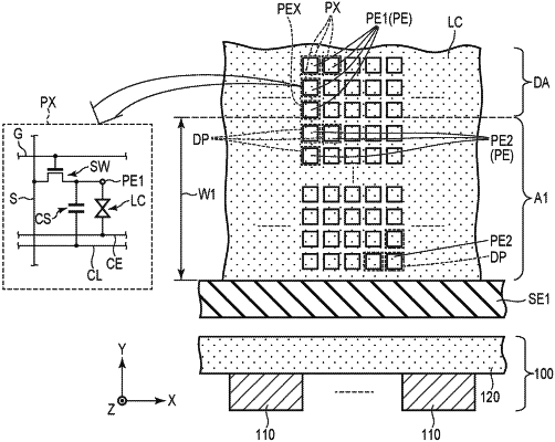
the liquid crystal layer is arranged over a display area where an image is displayed, a first area between the display area and the first portion, and a second area between the display area and the second portion, in plan view,
a first width of the first area is larger than a width of the second area,
the first substrate comprises a switching element arranged in the display area, and a feed line arranged in the first area and having a same potential as the common electrode,
the plurality of pixel electrodes include a first pixel electrode arranged in the display area, and a second pixel electrode arranged in the first area,
the first pixel electrode is electrically connected to the switching element, and
the second pixel electrode is electrically connected to the feed line.
|