| CPC G02F 1/025 (2013.01) [G02B 6/12 (2013.01); G02F 1/225 (2013.01); G02B 2006/12097 (2013.01); G02B 2006/12142 (2013.01); G02F 1/212 (2021.01); G02F 2201/063 (2013.01); G02F 2203/50 (2013.01)] | 20 Claims |
|
1. A phase-shifting device, comprising:
an insulating layer; and
a semiconductor waveguide layer disposed on the insulating layer and comprising:
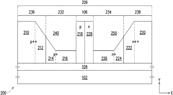
a waveguide portion having a p-n junction or p-i-n junction, the p-n junction or p-i-n junction comprising a p-doped portion and an n-doped portion disposed relative to each other along a first direction, the p-doped portion and n-doped portion each having an area with a first dimension along a second direction substantially parallel to the insulating layer and perpendicular to the first direction, and a second dimension along a third direction substantially perpendicular to the insulating layer and the first direction; and
a pair of slab portions, each adjacent to, and extending from, a corresponding one of the p-doped and n-doped portions in the first direction and having a cross-sectional area substantially parallel to the area of the corresponding one of the p-doped and n-doped portions, the cross-sectional area varying in size with distance from the corresponding one of the p-doped and n-doped portions along the first direction, the slab portion adjacent the p-doped portion of the p-n or p-i-n junction being p-doped having a p-dopant concentration higher than that of the p-doped portion, and the slab portion adjacent the n-doped portion of the p-n or p-i-n junction being n-doped and having an n-dopant concentration higher than that of the n-doped portion,
each of the pair of the slab portions having a top surface opposite the insulating layer from across the slab portion, the top surface comprising a sloped planar portion oriented at an oblique angle relative to the insulating layer and along a crystallographic plane.
|