| CPC G02F 1/025 (2013.01) | 12 Claims |

|
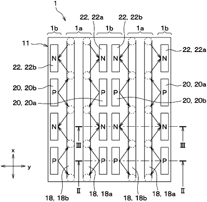
1. A phase shifter comprising:
a substrate including
a plurality of optical waveguide regions, and
a plurality of contact regions, each of which has a plurality of contact portions; and
a plurality of waveguides disposed at the substrate, each of which is configured to accumulate carriers to modulate a phase of light for guiding propagation of the light; and
a wiring portion configured to electrically connect each of the waveguides and each of the contact portions,
wherein each of the contact portions connecting one of the waveguides to one of electrodes to inject the carriers into the one of the waveguides,
wherein each of the waveguides has a lengthwise direction defined as a first direction,
wherein a direction that is perpendicular to the first direction and parallel to a surface of the substrate is defined as a second direction,
wherein the optical waveguide regions and the contact regions are disposed to be alternately aligned along the second direction,
wherein two of the waveguides are disposed at each of the optical waveguide regions, and the two of the waveguides are respectively a first waveguide and a second waveguide,
wherein the first waveguide is adjacent to one of the contact regions at a side of each of the optical waveguide regions facing the second direction, and the second waveguide is adjacent to another one of the contact regions at another side of each of the optical waveguide regions facing the second direction,
wherein each of the contact regions includes:
a first p-type contact portion as one of the contact portions that is made of a p-type semiconductor;
a first n-type contact portion as one of the contact portions that is made of an n-type semiconductor;
a second p-type contact portion as one of the contact portions that is made of the p-type semiconductor; and
a second n-type contact portion as one of the contact portions that is made of the n-type semiconductor,
wherein the first p-type contact portion and the first n-type contact portion are connected to one of the electrodes to inject the carriers into the first waveguide, and
wherein the second p-type contact portion and the second n-type contact portion are connected to another one of the electrodes to inject the carriers into the second waveguide.
|