US 11,988,874 B2
Data processing systems including optical communication modules
Peter Johannes Winzer, Aberdeen, NJ (US); Clinton Randy Giles, Watchung, NJ (US); Guilhem de Valicourt, Jersey City, NJ (US); and Peter James Pupalaikis, Ramsey, NJ (US)
Assigned to Nubis Communications, Inc., New Providence, NJ (US)
Filed by Nubis Communications, Inc., Aberdeen, NJ (US)
Filed on Oct. 6, 2021, as Appl. No. 17/495,338.
Claims priority of provisional application 63/088,914, filed on Oct. 7, 2020.
Claims priority of provisional application 63/210,437, filed on Jun. 14, 2021.
Claims priority of provisional application 63/245,005, filed on Sep. 16, 2021.
Claims priority of provisional application 63/116,660, filed on Nov. 20, 2020.
Claims priority of provisional application 63/146,421, filed on Feb. 5, 2021.
Claims priority of provisional application 63/145,368, filed on Feb. 3, 2021.
Claims priority of provisional application 63/159,768, filed on Mar. 11, 2021.
Claims priority of provisional application 63/225,779, filed on Jul. 26, 2021.
Claims priority of provisional application 63/175,021, filed on Apr. 14, 2021.
Claims priority of provisional application 63/208,759, filed on Jun. 9, 2021.
Claims priority of provisional application 63/173,253, filed on Apr. 9, 2021.
Claims priority of provisional application 63/245,011, filed on Sep. 16, 2021.
Claims priority of provisional application 63/178,501, filed on Apr. 22, 2021.
Claims priority of provisional application 63/192,852, filed on May 25, 2021.
Claims priority of provisional application 63/223,685, filed on Jul. 20, 2021.
Prior Publication US 2022/0244465 A1, Aug. 4, 2022
Int. Cl. G02B 6/36 (2006.01); G02B 6/38 (2006.01); G02B 6/42 (2006.01); H05K 1/02 (2006.01); H05K 1/14 (2006.01)
CPC G02B 6/3608 (2013.01) [G02B 6/3825 (2013.01); G02B 6/3869 (2013.01); H05K 1/0274 (2013.01); H05K 1/141 (2013.01); G02B 6/42 (2013.01); H05K 1/0206 (2013.01)] 92 Claims
OG exemplary drawing
 
1. An apparatus comprising:
at least one of a circuit board or a substrate;
a data processor unit mounted on a first side of the circuit board or the substrate; and
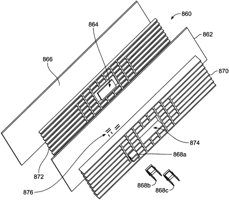
a first structure attached to a second side of the circuit board or the substrate, in which the second side of the circuit board or the substrate comprises a two-dimensional arrangement of second electrical contacts, the first structure is configured to be mechanically coupled to an optical module that has a two-dimensional arrangement of first electrical contacts;
wherein the first structure comprises walls that define a first opening, the walls also define one or more retaining mechanisms such that when the optical module is inserted into the first opening, the one or more retaining mechanisms on the walls of the first structure engage one or more latch mechanisms on the optical module to secure the optical module to the first structure, and the first electrical contacts on the optical module are electrically coupled to the second electrical contacts on the circuit board or the substrate.