| CPC G02B 6/1225 (2013.01) [C30B 25/04 (2013.01); C30B 29/403 (2013.01); H01L 21/02642 (2013.01); G02B 2006/1213 (2013.01); G02B 2006/12178 (2013.01)] | 16 Claims |
|
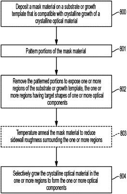
1. A method comprising:
depositing a mask material on a substrate or growth template, the substrate or growth template compatible with crystalline growth of a crystalline optical material;
removing patterned portions of the mask material to expose two or more regions of the substrate or growth template, the two or more regions having target shapes of two or more optical components and a gap between the two or more regions; and
selectively growing the crystalline optical material in the two or more regions to form the two or more optical components, the gap facilitating evanescent coupling between the two or more optical components.
|