| CPC G02B 6/12004 (2013.01) [G02B 6/424 (2013.01); G02B 6/4244 (2013.01); G02B 6/4245 (2013.01); G02B 2006/12102 (2013.01); G02B 6/30 (2013.01); G02B 6/4206 (2013.01)] | 11 Claims |
|
1. A package structure, comprising:
a substrate;
a chip which has an optical waveguide structure and an optical module recessed portion, the optical waveguide structure being adjacent to the optical module recessed portion, the optical module recessed portion facing the substrate, the chip being engaged to the substrate by flip chip; and
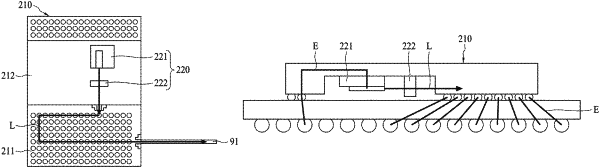
an optical module which is provided in the optical module recessed portion of the chip, wherein the optical module comprises a light source and a lens, the light source generates a light that passes through the lens and is emitted to the optical waveguide structure that is enclosed in the chip, and wherein an optical path of the light is located on a plane that is substantially parallel to the substrate, and a first electrical signal path of the optical module is different from a second electrical signal path of the chip,
wherein the chip is connected with an optical waveguide connection assembly, the substrate has an optical waveguide connection assembly recessed portion, and the optical waveguide connection assembly extends into the optical waveguide connection assembly recessed portion; and
wherein the optical waveguide connection assembly is connected with the chip in form of being suspended, to make the optical waveguide connection assembly separate from the substrate.
|