| CPC G02B 6/0056 (2013.01) [G02B 6/004 (2013.01); G02B 6/0051 (2013.01); G02B 6/0055 (2013.01); G02F 1/13362 (2013.01); G02F 1/136222 (2021.01); G02F 1/1368 (2013.01)] | 9 Claims |
|
1. A liquid crystal panel, comprising:
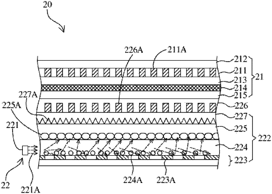
a backlight module and an array substrate facing each other,
wherein the array substrate comprises an outer glass, a quantum dot color filter, a liquid crystal layer, and a substrate, and
the backlight module comprises a light source and a polarizing sheet, wherein the light source is adjacent to the polarizing sheet,
the polarizing sheet comprises a reflecting sheet, a light guide plate disposed on the reflecting sheet, and a diffusion sheet disposed on the light guide plate,
the light guide plate comprises a plurality of dots formed by the nano-imprinting, each dot of the plurality of dots has a size between 0.1 mm and 1 mm, a pitch between every two adjacent dots of the plurality of dots is between 0.1 mm and 10 mm, and
the light source is adjacent to the light guide plate; and
a first metal wire gate layer disposed on the array substrate, between the backlight module and the substrate of the array substrate and away from the liquid crystal layer, wherein the first metal wire gate layer is formed through nano-imprinting to have a thickness greater than zero and less than or equal to 0.1 mm, the first metal wire gate layer comprises a plurality of first metal wires, a distance between every two adjacent first metal wires of the plurality of first metal wires is greater than zero and less than 10 nm, each of the plurality of first metal wires has a width greater than zero and less than 10 nm, and the first metal wire gate layer comprises at least one of aluminum, iron, copper, chromium, silver, and gold;
wherein the array substrate further comprises a second metal wire gate layer, the second metal wire gate layer is a built-in polarizing sheet formed by the nano-imprinting, and
the outer glass, the quantum dot color filter, the second metal wire gate layer, the liquid crystal layer, and the substrate are arranged in sequence.
|