US 11,988,858 B2
Optical film device
Robert M. Jennings, Shoreview, MN (US); Jo A. Etter, Stillwater, MN (US); Susan L. Kent, Shorewood, MN (US); Erin A. McDowell, Afton, MN (US); Timothy L. Wong, West St. Paul, MN (US); and Zhisheng Yun, Sammamish, WA (US)
Assigned to 3M INNOVATIVE PROPERTIES COMPANY, St. Paul, MN (US)
Filed by 3M INNOVATIVE PROPERTIES COMPANY, St. Paul, MN (US)
Filed on Sep. 7, 2022, as Appl. No. 17/939,183.
Application 17/939,183 is a division of application No. 15/733,257, granted, now 11,467,329, previously published as PCT/IB2019/051262, filed on Feb. 15, 2019.
Claims priority of provisional application 62/632,033, filed on Feb. 19, 2018.
Prior Publication US 2023/0003929 A1, Jan. 5, 2023
Int. Cl. G02B 5/30 (2006.01); G02B 5/10 (2006.01); G02B 27/01 (2006.01); G02B 3/00 (2006.01)
CPC G02B 5/3033 (2013.01) [G02B 5/10 (2013.01); G02B 5/3041 (2013.01); G02B 5/3066 (2013.01); G02B 27/0172 (2013.01); G02B 2003/0093 (2013.01); G02B 2027/013 (2013.01)] 1 Claim
OG exemplary drawing
 
1. A device, comprising:
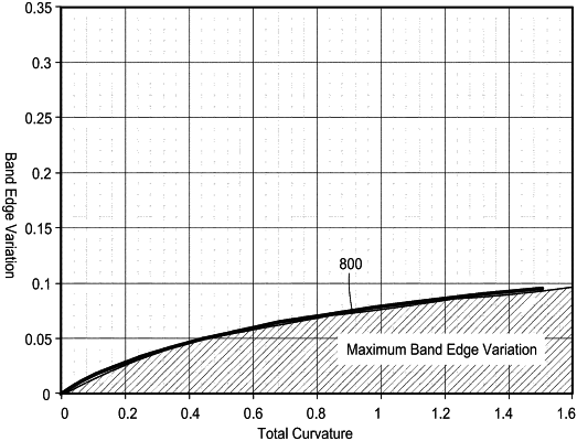
at least one optical film and having an active area that is curved in two orthogonal directions such that the active area has a total curvature, C, greater than 0.1, the active area having a minimum pass band edge, λEmin, a maximum pass band edge, λEmax, an average pass band edge, λave, wherein a variation in upper pass band edge, (λEmax−λEmin)/λEave, in the active area is less than ln[1+(12/π)C]/20.