| CPC G02B 1/118 (2013.01) [B32B 5/16 (2013.01); B32B 7/12 (2013.01); B32B 17/10018 (2013.01); B32B 27/14 (2013.01); B32B 2264/102 (2013.01)] | 12 Claims |
|
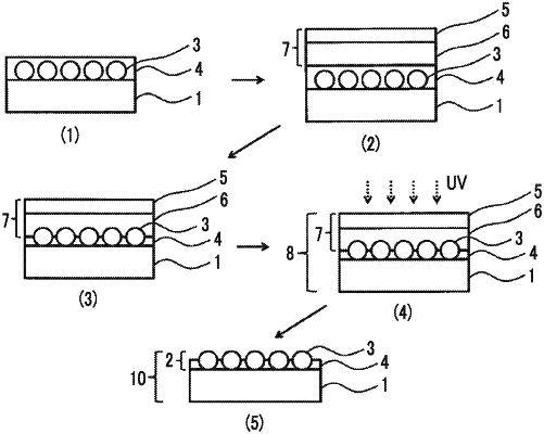
1. A method of manufacturing an antireflection product, comprising, in order:
a step (1) of providing a binder compound and a particle (a2) having an average primary particle diameter of 100 nm to 380 nm on a substrate, in a thickness in which the particle (a2) is buried in a layer (a) including the binder compound;
a step (2) of bonding a layer (b) of a pressure sensitive film having a support and the layer (b) including a pressure sensitive adhesive on the support to the layer (a);
a step (3) of causing a position of an interface between the layer (a) and the layer (b) to move toward the substrate such that the particle (a2) is buried in layers obtained by combining the layer (a) and the layer (b) and protrudes from the layer (a) at the interface;
a step (4) of curing the layer (a) in a state in which the particle (a2) is buried in the layers obtained by combining the layer (a) and the layer (b); and
a step (5) of peeling off the pressure sensitive film.
|