| CPC G02B 1/04 (2013.01) [B24B 37/08 (2013.01); G02B 6/262 (2013.01); G02B 2027/0125 (2013.01); G02B 27/0172 (2013.01)] | 14 Claims |
|
1. A method of producing an optical member comprising an organic polymer, the method comprising:
a step of preparing a molded member including the organic polymer,
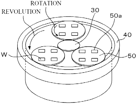
a first polishing step of polishing the molded member with a polishing pad, after arranging the molded member in a movement restriction member which restricts the movement of the molded member during the polishing of the molded member, and
a second polishing step of polishing the molded member after being subjected to the first polishing step, with a suede type polishing pad in which a nap layer is provided and a polishing liquid containing an abrasive material made of alumina,
wherein, in the first polishing step, the molded member is polished using an abrasive material having a grain size of 3 μm or more and the optical member is produced from the molded member by the first polishing step and the second polishing step,
wherein the optical member comprises a surface A which has an area of 1 mm2 or more, and in which a flatness of a region having an area of 1 mm2, as measured by a non-contact type optical flatness meter, is 80 μm or less, a plurality of linear marks having a height of 50 nm or less are observed, in an image of a region having an area of 4,200 μm2 in the surface A, when the region is imaged by a non-contact type optical surface roughness tester, and the plurality of the linear marks are polishing marks.
|