| CPC G01S 7/493 (2013.01) [G01B 11/22 (2013.01); G01S 17/894 (2020.01); G06T 5/20 (2013.01); G06T 7/521 (2017.01)] | 24 Claims |
|
1. A device comprising circuitry configured to:
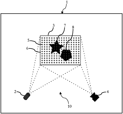
obtain image data of a scene being representative of a time of flight measurement of light reflected from the scene, wherein the image data is based on a pattern of light being illuminated on the scene, wherein the pattern of light includes high intensity light areas and low intensity light areas;
obtain, based on the image data, first image data being representative of the high intensity light areas;
obtain, based on the image data, second image data being representative of the low intensity light areas;
estimate direct component image data based on the first image data and the second image data; and
generate an output depth map of the scene based on the direct component image data and the second image data, comprising:
converting the direct component image data to a first depth map;
converting the second image data to a second depth map, the second depth map having a higher resolution than the first depth map; and
using the first depth map and the second depth map to generate the output depth map.
|