| CPC G01R 31/392 (2019.01) [H01M 10/44 (2013.01); H01M 10/48 (2013.01); H02J 7/005 (2020.01); H01L 29/7869 (2013.01); H01M 2220/20 (2013.01)] | 8 Claims |
|
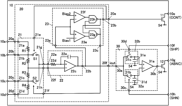
1. A semiconductor device comprising a first circuit and a second circuit,
wherein the first circuit comprises a power gauge and an anomalous current detection circuit,
wherein the power gauge comprises a current divider circuit and an integrator circuit,
wherein the anomalous current detection circuit comprises a first memory, a second memory, and a first comparator,
wherein the integrator circuit is configured to convert a detection current detected at the current divider circuit into a detection voltage by integrating the detection current,
wherein the anomalous current detection circuit is configured to be supplied with the detection voltage, a first signal at a first time, and a second signal at a second time,
wherein the anomalous current detection circuit is configured to store the detection voltage at the first time in the first memory using the first signal,
wherein the anomalous current detection circuit is configured to store the detection voltage at the second time in the second memory using the second signal, and
wherein the first comparator is configured to output a change from the detection voltage at the first time to the detection voltage at the second time as a first output signal to the second circuit.
|