| CPC G01R 31/318541 (2013.01) | 19 Claims |
|
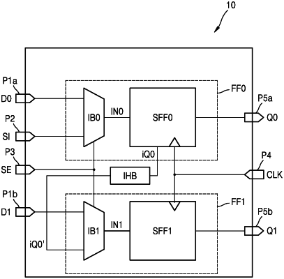
1. A multi-bit flip-flop comprising:
a scan input pin;
a first data input pin;
a second data input pin;
a first output pin;
a second output pin;
a first flip-flop arranged on a first row, including a first input buffer electrically connected with the scan input pin and the first data input pin, and a first output driver electrically connected with the first output pin;
a second flip-flop arranged on a second row different than the first row, including a second input buffer electrically connected with the second data input pin, and a second output driver electrically connected with the second output pin;
an internal hold buffer electrically connected to the first output driver on the first row and the second input buffer on the second row; and
a scan enable pin configured to receive a scan enable signal indicative of a scan mode,
wherein the internal hold buffer is configured to provide a scan output of the first flip-flop to the second flip-flop in the scan mode,
wherein the internal hold buffer is arranged adjacent to the first output driver on the first row,
wherein the first flip-flop further comprises:
a first feedback driver configured to generate a first feedback signal based on a scan input signal output from the scan input pin, the scan enable signal, and a first dynamic feedback signal;
a first dynamic logic driver arranged adjacent to the first feedback driver, and configured to generate the first dynamic feedback signal based on a first data input signal output from the first data input pin, the scan enable signal, and the first feedback signal; and
a first static latch arranged adjacent to the first dynamic logic driver, and configured to output a first internal signal generated based on the first dynamic feedback signal to the internal hold buffer and the first output driver.
|