| CPC G01R 31/14 (2013.01) [G01R 31/2642 (2013.01)] | 14 Claims |
|
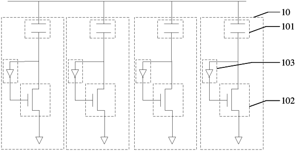
1. A test circuit, comprising:
M test units, each test unit having a first terminal and a second terminal, the first terminal of each test unit being connected to a power wire, the second terminal of each test unit being connected to a ground wire, M being a positive integer;
each test unit comprises a time dependent dielectric breakdown (TDDB) test component, a switch, and a control circuit, wherein each TDDB test component has a first resistance value before being broken down, each TDDB test component has a second resistance value after being broken down, the first resistance value is greater than the second resistance value, a first terminal of each TDDB test component is the first terminal of the test unit and a second terminal of each TDDB test component is connected to a first terminal of each switch, a second terminal of each switch is the second terminal of the test unit, and the first terminal of each switch is connected to a control terminal of each switch through each control circuit.
|